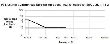
G.8262 (clause 9.2): Where did the Jitter Tolerance mask for 1G Electrical interfaces come from?
G.8262 does not specify a jitter tolerance mask for 1G electrical interfaces (Table 6, note 2 and Table 11, note 1 both state that these interfaces are “for further study”). However, the 4-lane, multi-level physical layer scheme used for 1G electrical Ethernet has a clock rate of 125MHz (versus 1.25GHz for 1Gbit/s optical Ethernet), which implies a 10:1 ratio for jitter parameters. We have therefore implemented 1G electrical Ethernet jitter testing using a scaled jitter tolerance mask to an upper frequency of 5kHz and a jitter generation measurement filter of 250Hz to 1MHz using this implied ratio.
Mapping between SyncE jitter period and UI give us:
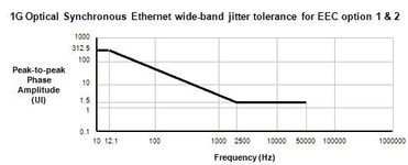
- 1G optical: clock rate = 1.25GHz and so one UI = 0.8ns
- 1G electrical: clock rate = 125MHz and so one UI = 8ns
The 1G optical mask is:
From this mask, we derived an equivalent for 1G electrical as follows:
The 10Hz point must aligns with the G.8262 10Hz wander tolerance limit, which is 250ns. 250ns equates to 31.25UI. We then simply scaled the higher-frequency breakpoints and max frequency down by a factor of ten (because the clock rate is 1/10 compared to 1G optical). Since UI is already a normalised unit, we retained the 1.5UI requirement at the higher frequencies
This gives us: